2-30
X8SIL/X8SIL-F User's Manual
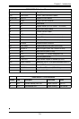
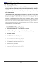
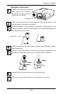
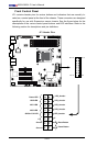
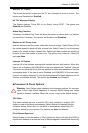
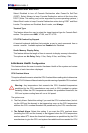
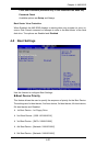
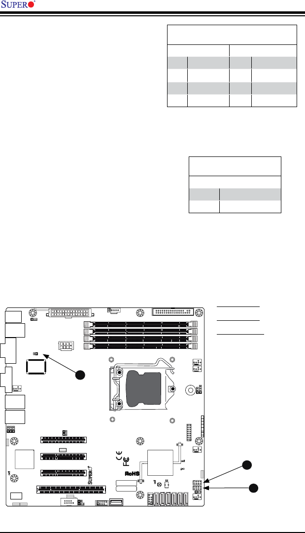
Serial_Link-SGPIO
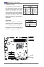
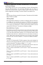
PinDenitions
Pin# Denition Pin Denition
1 NC 2 NC
3 Ground 4 DATA Out
5 Load 6 Ground
7 Clock 8 NC
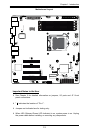
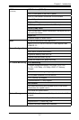
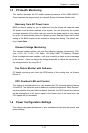
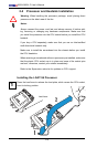
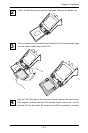
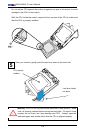
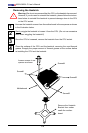
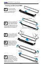
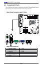
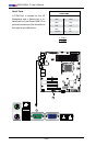
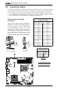
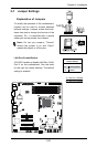
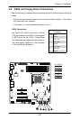
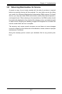
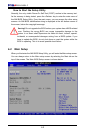
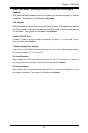
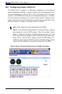
T-SGPIO 0/1 Headers
Two T-SGPIO (Serial-Link General Pur-
pose Input/Output) headers are located
near the SATA connectors on the moth-
erboard. These headers are used to
communicate with the enclosure manage-
ment chip in the system. See the table on
the right for pin denitions. Refer to the
board layout below for the locations of
the headers.
NC: No Connections
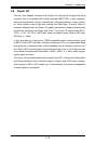
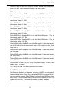
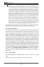
A. T-SGPIO 0
B. T-SGPIO 1
C. Alarm Reset
C
A
B
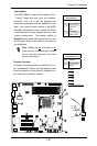
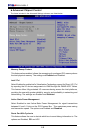
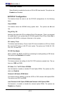
Alarm Reset
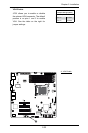
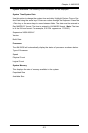
If three power supplies are installed and
Alarm Reset (JAR) is connected, the sys-
tem will notify you when any of the three
power modules fail. Connect JAR to a
micro-switch to turn off the alarm that is
activated when a power module fails. See
the table on the right for pin denitions.
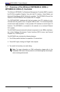
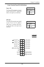
Alarm Reset
PinDenitions
Pin Setting Denition
Pin 1 Ground
Pin 2 +5V
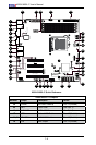
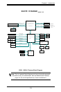
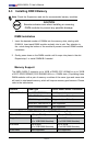
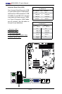
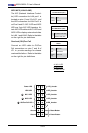
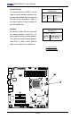
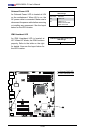
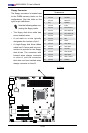
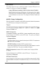
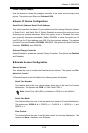
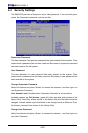
MAC CODE
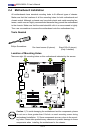
JPI2C
JF1
JPW1
U26
J8
J6
J5
J14
1
J13
U61
T-SGPIO1
T-SGPIO2
J24
JLAN2
JLAN1
SPKR1
JBT1
1
JI2C1
1
JI2C2
1
JL1
LE4
LE2
LE3
LE7
JPT1
1
JPB
JLED1
1
1
JPUSB1
1
JPL1
1
JPL2
JPG1
JD1
1
FAN2
FAN1
FAN5
1
FAN4
FAN3
J16
PCI1
U2
BAR CODE
1-2:ENABLE
2-3:DISABLE
JPL2:LAN2 JPL1:LAN1
2-3:DISABLE
1-2:ENABLE
JPB:BMC
JPI2C:PWR I2C
JD1:Buzzer/Speaker
COM2
FLOPPY
DDR3 1066/1333 UDIMM/RDIMM required
VGA
COM1
USB4
JBT1:CMOS CLEAR
SLOT7 PCI-E X8 GEN2
JPT1:TPM
JL1
LAN1
JPUSB1:B/P USB WAKE UP
1-2:ENABLE
2-3:DISABLE
DIMM2B
DIMM2A
USB 10/11
JI2C1/JI2C2
USB2/3
SLOT6 PCI-E X8 GEN2
2-3:Disable
1-2:Enable
JAR:
PSU ALARM RST
CPU
JLED1:Power LED
OFF:Disable
ON:Enable
2-3:Disable
1-2:Enable
REV:1.00
X8SIL
DESIGNED IN USA
2-3:DISABLE
1-2:ENABLE
:CHASSIS INTRUSION
JF1
ON
LED LED
PWRHDD
NIC1
NIC2
OH/FFXRST
PWR
I-SATA3
I-SATA4
I-SATA2
I-SATA1
I-SATA0
I-SATA5
SLOT5 PCI-E X4 on X8
SLOT4 PCI 33MHZ
KB/MOUSE
DIMM1B
JPG1: VGA
DIMM1A
JAR