Chapter 3 Signal Connections
BNC-2140 User Manual 3-4
©
National Instruments Corporation
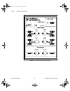
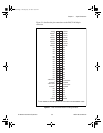
Note This BNC-2140 pin assignment maps to the pin assignment of the DSA device you
are connecting to the BNC-2140. Refer to your DSA device user manual for the
pin assignments specific to your device connection.
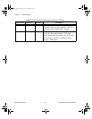
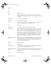
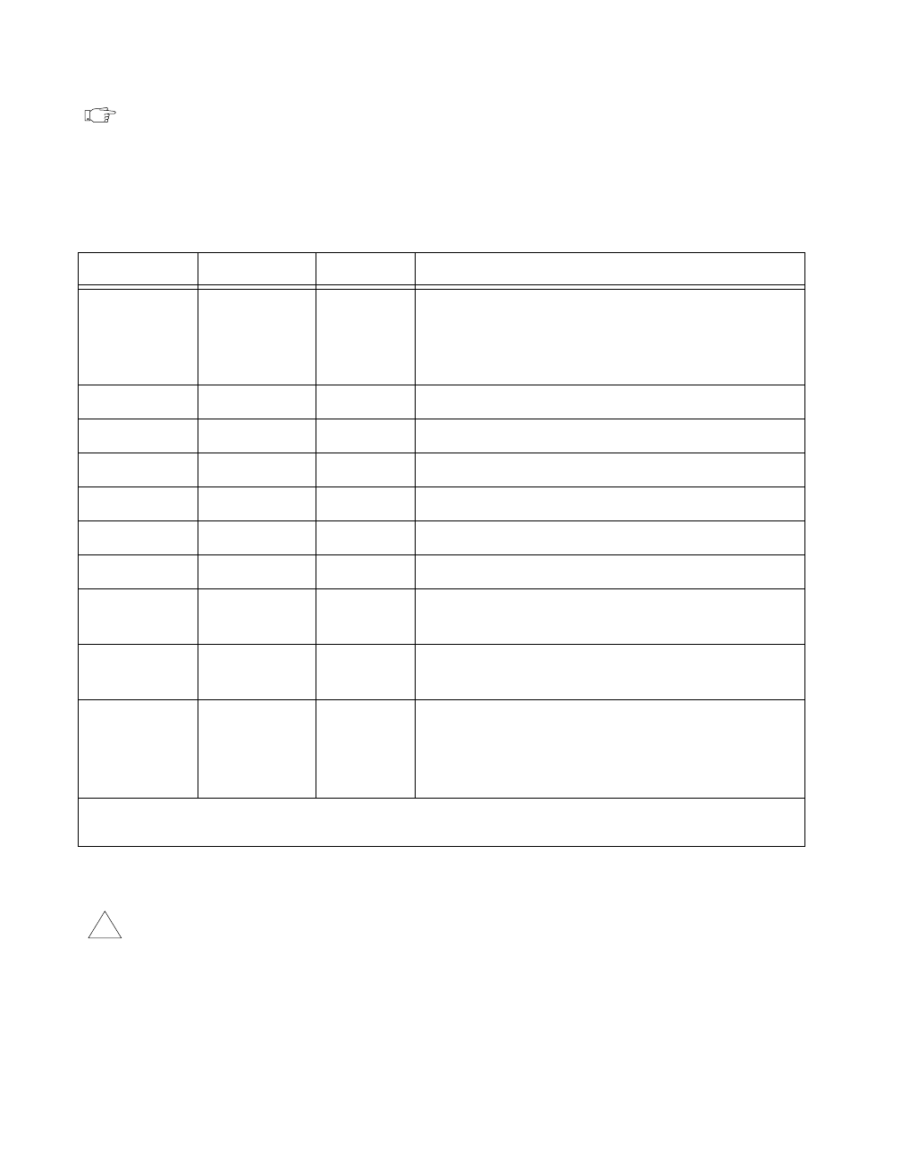
Table 3-2 shows the pin assignments for the internal 68-pin I/O connector.
Refer to Figure 3-1 for the pin assignments for the 68-pin connector.
Caution Connections that exceed any of the maximum ratings of input or output signals
on the BNC-2140 accessory can damage not only the BNC-2140, but also the DSA
plug-in device and the computer as well. Maximum input ratings for each signal
are given in Appendix A, Specifications. National Instruments is not liable for any
damages resulting from signal connections exceeding maximum ratings.
Table 3-2. 68-Pin Analog I/O Connector Signal Descriptions
Signal Name Reference Direction Description
AIGND — — Analog Input Ground—These pins are the reference
point for single-ended measurements in SE mode
and the bias current return point for differential
measurements.
+ACH<0..3> AIGND Input +Analog Input Channel 0 through 3.
–ACH<0..3> AIGND Input
–Analog Input Channel 0 through 3.
+DAC0OUT –DAC0OUT Output +Analog Output Channel 0.
–DAC0OUT +DAC0OUT Output
–Analog Output Channel 0.
+DAC1OUT –DAC1OUT Output +Analog Output Channel 1.
–DAC1OUT +DAC1OUT Output
–Analog Output Channel 1.
AOGND — — Analog Output Ground—The analog output
voltages are ultimately referenced to this node.
DGND — — Digital Ground—This pin supplies the reference for
the +5 VDC supply.
+5 V DGND Output +5 VDC Source—These pins are fused for up to
0.5 A of +5 V supply on the DSA plug-in device.
The fuse is self-resetting. This source powers the
ICP circuits of the BNC-2140.
NOTE:
For +ACH<0..3>, –ACH<0..3>, +DAC0OUT, –DAC0OUT, +DAC1OUT, and –DAC1OUT descriptions see
Table 3-1.
!
UM.book Page 4 Tuesday, July 14, 1998 10:37 AM