2-26
X8STi/X8STi-F/X8STi-3F/X8STi-LN4 User's Manual
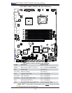
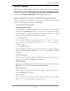
LSI 1068E
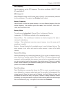
NIC4 LED
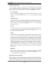
JBMC1
Serial_Link-SGPIO
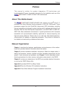
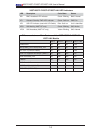
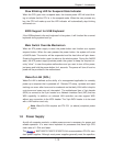
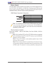
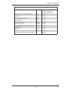
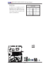
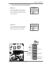
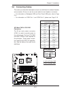
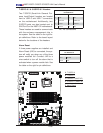
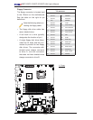
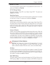
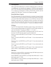
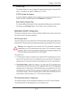
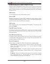
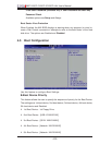
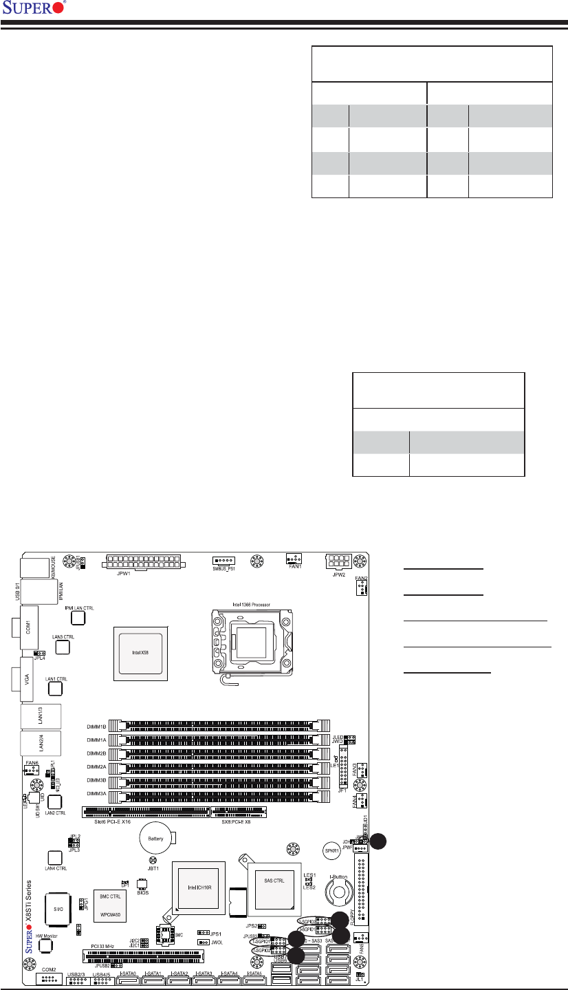
Pin Defi nitions
Pin# Defi nition Pin Defi nition
1NC 2 NC
3 Ground 4 DATA Out
5 Load 6 Ground
7 Clock 8 NC
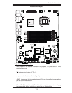
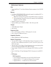
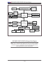
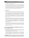
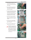
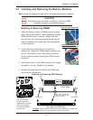
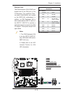
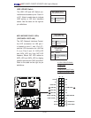
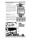
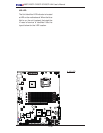
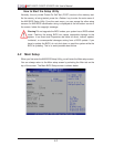
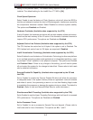
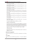
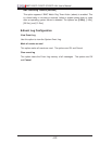
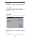
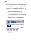
T-SGPIO 0/1 & 3-SGPIO 0/1 Headers
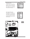
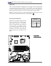
Two T-SGPIO (Serial-Link General Pur-
pose Input/Output) headers are located
next to USB 6 and USB 7 connectors
on the motherboard. Additionally, two
3-SGPIO ports are also located next to
SAS Port 3 on the X8STi-3F motherboard.
These headers are used to communicate
with the enclosure management chip in
the system. See the table on the right for
pin defi nitions. Refer to the board layout
below for the locations of the headers.
NC: No Connections
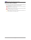
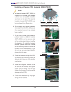
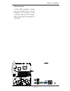
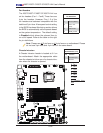
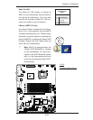
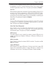
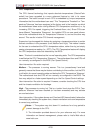
A. T-SGPIO 0
B. T-SGPIO 1
C.3-SGPIO 0 (X8STi-3F)
D. 3-SGPIO 1 (X8STi-3F)
E. Alarm Reset
C
D
A
B
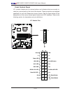
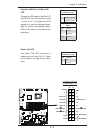
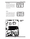
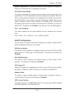
Alarm Reset
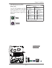
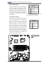
If three power supplies are installed and
Alarm Reset (JAR) is connected, the sys-
tem will notify you when any of the three
power modules fail. Connect JAR to a
micro-switch to turn off the alarm that is
activated when a power module fails. See
the table on the right for pin defi nitions.
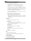
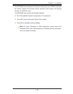
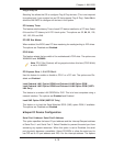
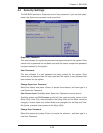
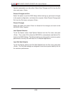
Alarm Reset
Pin Defi nitions
Pin Setting Defi nition
Pin 1 Ground
Pin 2 +5V
E