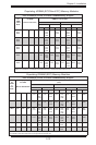
2-26
X9DRG-HF/X9DRG-HTF Motherboard User’s Manual
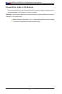
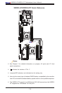
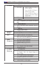
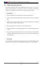
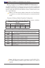
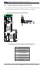
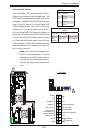
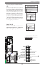
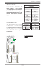
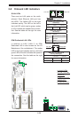
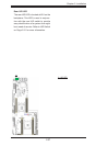
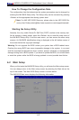
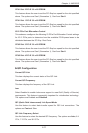
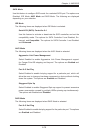
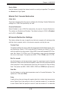
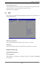
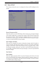
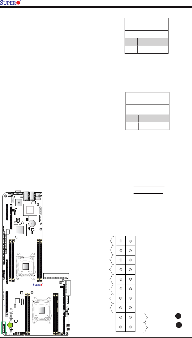
Power Button
The Power Button connection is located
on pins 1 and 2 of JF1. Momentarily
contacting both pins will power on/off
the system. This button can also be con-
gured to function as a suspend button
(with a setting in the BIOS - See Chapter
5). To turn off the power when the system
is in suspend mode, press the button for
4 seconds or longer. Refer to the table on
the right for pin denitions.
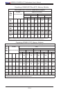
Power Button
PinDenitions(JF1)
Pin# Denition
1 Signal
2 Ground
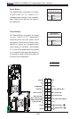
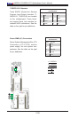
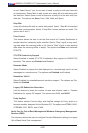
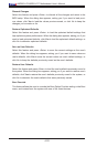
Reset Button
The Reset Button connection is located
on pins 3 and 4 of JF1. Attach it to a
hardware reset switch on the computer
case. Refer to the table on the right for
pin denitions.
Reset Button
PinDenitions(JF1)
Pin# Denition
3 Reset
4 Ground
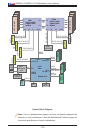
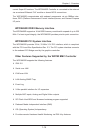
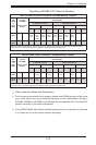
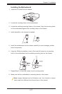
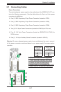
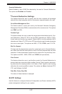
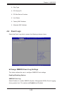
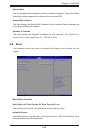
A. Reset Button
B. PWR Button
A
B
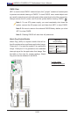
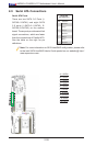
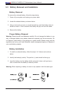
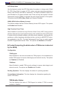
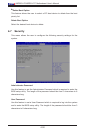
Power Button
Blue+ (OH/Fan Fail/
PWR FaiL/UID LED)
1
NIC1 Link LED
Reset Button
2
Power Fail LED
HDD LED
FP PWRLED
Reset
PWR
3.3 V
ID_UID_SW/3/3V Stby
Red+ (Blue LED Cathode)
Ground
Ground
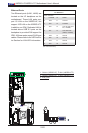
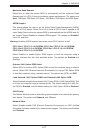
1920
3.3V
X
Ground
NMI
X
NIC2 Link LED
NIC2 Activity LED
NIC1 Activity LED
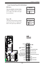
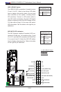
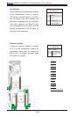
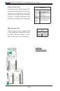
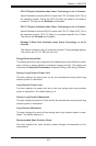
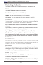
JPCIE6
JSD1
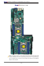
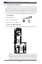
X9DRG-HF
LE4
SW1
JPW10
JLAN2
JLAN1
JRK1
JI2C2
JI2C1
JOH1
JSPK1
JL1
JBT1
J21
JCOM1
JPCIE1
JPCIE2
JPCIE3
JPCIE4
JPCIE5
JPW11
JPW3
JPW4
JPW5
JPW7
JPW8
JVGA1
JPW9
JPW1
I-SATA0
S-SATA0
S-SATA1
S-SATA2
S-SATA3
DM1
LE1
DM2
JPL1
JWD1
J30
JPB1
J29
JPBR1
JPME1
JWP1
JPG1
FAN2
FAN1
FANF
FAND
FANH
FANC
FANG
FANE
FAN4
FAN3
FANA
FANB
T-SGPIO5
T-SGPIO1
T-SGPIO2
I-SATA3
I-SATA4
I-SATA5
JF1
JTPM1
JPW2
USB/0/1
IPMI LAN
PCH Slot6 PCI-E 2.0 x4
CPU1 Slot1 PCI-E 3.0 x8
PCI-E 3.0 X16
CPU2 Slot4 PCI-E 3.0 X16
CPU2 Slot 3 PCI-E 3.0 X16
CPU1Slot1PCI-E 3.0 X16
P2-DIMME
P2-DIMMF
P2-DIMMG
P2-DIMMH
P1-DIMMD
P1-DIMMC
P1-DIMMB
P1-DIMMA
BIOS
JPW6
PHY
I-SATA1
I-SATA2
Battery
S/IO
BMC CTRL
LAN CTRL
PCH
Rev.
1.20
(in x16)
(in x8)
CPU1 Slot2
JPME2
CPU1
CPU2