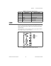
Chapter 2 Functional Overview
© National Instruments Corporation 2-3 PXI-8170 Series User Manual
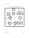
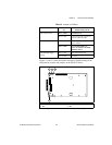
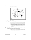
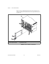
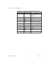
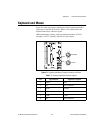
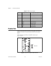
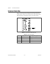
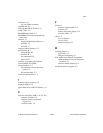
The PXI-8170 consists of the following logic blocks on the CPU module
and the I/O (daughter card) module. The CPU module has the following
logic blocks:
• Slot 1 CPU is the socket definition for the Intel Pentium II and III
processor families.
• The SO-DIMM block consists of two 64-bit SDRAM sockets that can
hold up to 128 MB each.
• The Chip Set North Bridge connects to the CPU, SDRAM, AGP port,
and PCI bus.
• The Chip Set South Bridge connects to the PCI bus USB, IDE, and ISA
ports.
• The AGP video circuitry is a 1x AGP-based design that has 2 MB of
video RAM. It also contains a TFT LCD Interface, which is used in the
National Instruments PXI-1020 and PXI-1025 chassis.
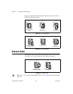
• The USB connector connects the chip set to the Universal Serial Bus
interface.
• The PXI connector connects the PXI-8170 to the PXI/CompactPCI
backplane.
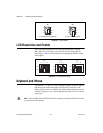
• The Keyboard/Mouse block contains the PS/2 keyboard and mouse
interface.
• The BIOS/RTC block contains the boot Basic Input Output System
(BIOS) and the Real Time Clock interface.
• The Watchdog Timer block is the circuitry that, once configured,
signals if the timer is not refreshed. Refer to the
drivers.txt file in
the
C:\Images\PXI8170 directory for more information on
configuring and using the watchdog timer.
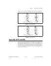
• The PC Peripherals blocks represent the other peripherals supplied by
the PXI-8170 Series. The PXI-8170 has one serial port, an ECP/EPP
parallel port, and a 1.44 MB, 3.5 in. floppy drive.
• The IDE block is dedicated PCI-IDE circuitry providing fast ATA-3
transfers to the internal hard drive. The IDE feature is built into the
chip set.
The I/O module has the following logic blocks:
• Internal 1.44 MB floppy drive
• 2.5 in. hard drive—4 GB or larger
• TFT LCD interface for PXI-1020 and PXI-1025 chassis