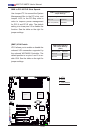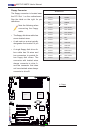
2-26
X8ST3-F/X8STE User's Manual
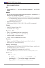
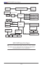
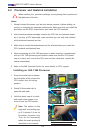
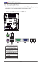
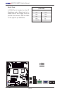
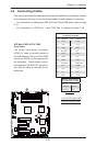
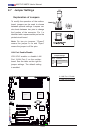
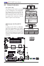
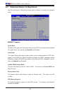
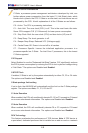
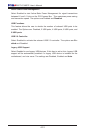
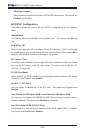
BMC JTAG
1
SAS1
SAS2
SAS7
SAS3
SAS4
SAS5
SAS6
JWOL
Battery
JD1
SPKR1
JAR
JI2C1
JI2C2
JPS2
JL1
1
JOH
1
JF1
LES1
LE1
COM1
FAN 4
FAN 3
FAN 5
FAN 2
FAN 1
JPW1
SMBUS_PS1
JPW2
JPG1
JPUSB3
JBMC1
JPS1
JPUSB2
JPL1
JPL2
JLED
JWD
JPUSB1
IPMI_LAN
COM2
Floppy
I-Button
T-SGPIO1
3-SGPIO2
3-SGPIO1
USB 6/7
USB 4/5
USB3
USB2
Slot6 PCI-E 2.0 X8 on X16
Slot3 PCI-E 2.0 X8
I-SATA4
I-SATA5
Slot4 PCI-E 2.0 X4 on X8
Slot2 PCI 33MHz
Slot5 PCI-E 2.0 X8
I-SATA2
I-SATA3
DIMM1B
DIMM1A
DIMM3B
DIMM2B
DIMM2A
DIMM3A
I-SATA0
I-SATA1
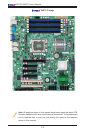
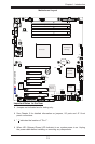
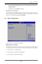
X8ST3-F/X8STE
USB 0/1
LAN2
LAN1
VGA
KB/MOUSE
BIOS
JBT1
Slot1 PCI 33MHz
SAS0
T-SGPIO2
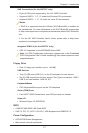
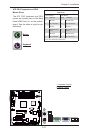
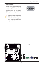
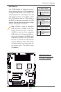
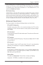
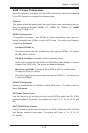
LAN CTRL
for IPMIl LAN
LAN
CTRL1
LAN
CTRL2
SI/O
BMC CTRL
BMC
Firmware
SAS CTRL
Intel ICH10R
South Bridge
Intel X58-Express
North Bridge
Intel Processor
LES2
LSI 1068E
WPCM 450
CPU FAN
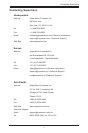
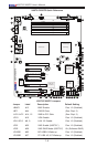
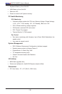
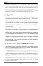
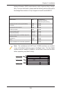
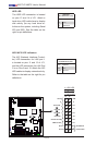
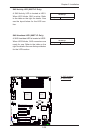
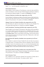
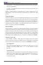
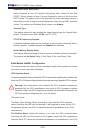
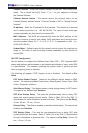
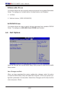
Serial_Link-SGPIO
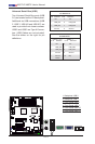
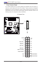
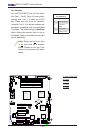
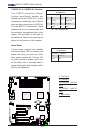
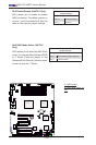
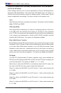
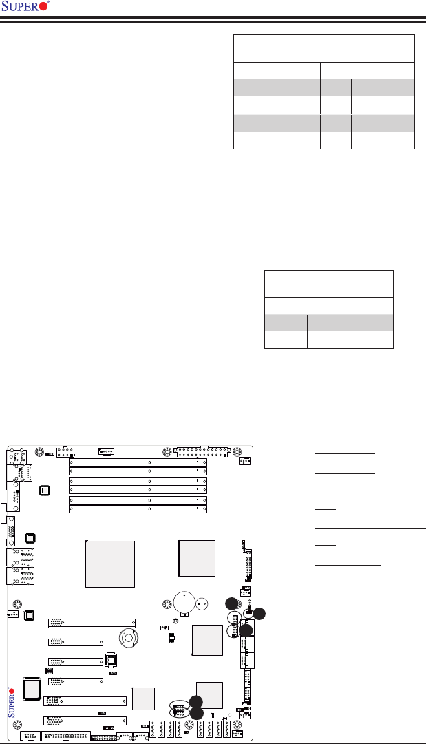
PinDenitions
Pin# Denition Pin Denition
1 NC 2 NC
3 Ground 4 DATA Out
5 Load 6 Ground
7 Clock 8 NC
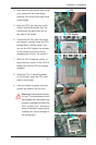
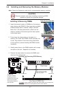
T-SGPIO 0/1 & 3-SGPIO 0/1 Headers
Two T-SGPIO (Serial-Link General
Purpose Input/Output) headers are
located next to the I-SATA Port 1 on the
motherboard. Additionally, two 3-SGPIO
ports are also located next to SAS Port
3 on the X8ST3-F motherboard. These
headers are used to communicate with
the enclosure management chip in the
system. See the table on the right for
pin denitions. Refer to the board layout
below for the locations of the headers.
NC: No Connections
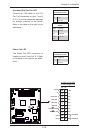
A. T-SPGIO 0
B. T-SPGIO 1
C.3-SPGIO 0 (X8ST3-F
only)
D. 3-SPGIO 1 (X8ST3-F
only)
E. Alarm Reset
C
D
A
B
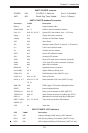
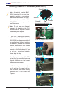
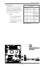
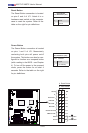
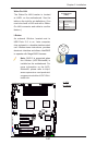
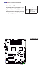
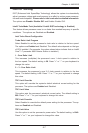
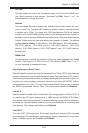
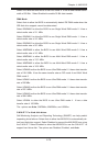
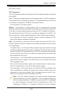
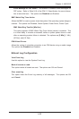
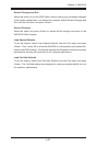
Alarm Reset
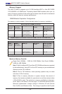
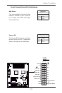
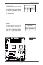
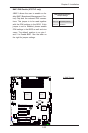
If three power supplies are installed
and Alarm Reset (JP5) is enabled, the
system will notify you when any of the
three power modules fail. Connect JP5
to a micro-switch to enable you to turn
off the alarm that is activated when a
power module fails. See the table on the
right for pin denitions.
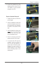
Alarm Reset
PinDenitions
Pin Setting Denition
Pin 1 Ground
Pin 2 +5V
E